
- Address
- Rm B306, Build A, RunFengYuan Business Center, Block 74, Baoan District , Shenzhen , China
- Phone
- 86-13534206421 / 86-0755-27788210
- nicolas.liu@samtronik.com
Semi-conductor loaders and unloaders are designed for handling lead frames, substrates, and fragile semiconductor packages, with higher precision cleaner environments and gentler handling compared to standard PCB handling equipment.
While standard PCB handling equipment is designed for rigid FR4 boards used in SMT assembly, semi-conductor handling equipment deals with more delicate, smaller, and often strip-based carriers used in semiconductor packaging. Key differences include: (1) Material handling — semi-conductor loaders handle lead frames, ceramic substrates, and BGA strip carriers instead of standard PCBs. (2) Cleanliness — semiconductor processes require Class 1000 or better cleanroom compatibility. (3) Precision — positioning accuracy must be in the sub-millimeter range to handle fine-pitch components. (4) Anti-static — more stringent ESD protection is required. (5) Magazine design — custom mags for lead frames or JEDEC trays. (6) Speed — typically slower but with greater positional accuracy. Samtronik's semi-conductor loaders incorporate ceramic guide rails, ionized air curtains, and Class 100 cleanroom-compatible construction. They handle a wide range of substrate formats including L/F (Lead Frame), MAP (Molded Array Package), and BGA substrates.


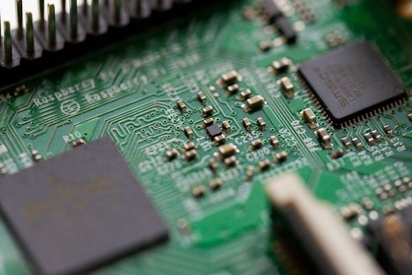
The global semiconductor equipment market continues to expand with packaging and assembly equipment seeing steady growth. Samtronik's semi-conductor loaders support substrate sizes from 50x50mm to 300x300mm with a positioning accuracy of ±0.05mm, and can process up to 5-8 strips per minute depending on magazine configuration.